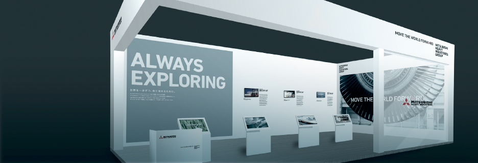
EVENTS & EXHIBITIONS SHARE Introduction of events and exhibitions that Mitsubishi Heavy Industries exhibits. What's News 2026-03-19 "Data Center World 2026" has been updated. 2026-02-16 "NVIDIA GTC 2026" has been updated. 2026-01-13 "JANOG57" has been updated. 2026-01-09 "PTC'26" has been updated. 2026-01-05 "2026 AHR Expo" has been updated. 2025-12-15 "SCA/HPCAsia 2026" has been updated. Main Events & Exhibitions Data Center World 2026 (Dates: April 20(Mon.) - 23(Thu.), 2026) NVIDIA GTC 2026 (Dates: March 16 (Mon.) - 19(Thu.), 2026) JANOG57 (Dates: February 11(Wed, National Holiday) - 13(Fri.), 2026) PTC'26 (Dates: January 18(Sun.) - 21(Wed.), 2026) 2026 AHR Expo (Dates: February 2(Mon.) - 4(Wed.), 2026) SCA/HPCAsia 2026(Dates: January 26(Mon.) - 29(Thu.), 2026) Supercomputing 2025 (Dates:November 16(Sun.) - 21(Fri.), 2025) Data Centre World Asia 2025 (Dates:October 8(Wed.) - 9(Thu.), 2025) About Us Company Overview Philosophy Corporate Policy Corporate Profile Officers Corporate Organization History Exhibition Facilities Event & Exhibition MHI Group’s Declaration to achieve Carbon Neutral by 2040 CEO Message Outline of MHI Group Business Area Global Network Locations Procurement REGIONS Mitsubishi Minatomirai Industrial Museum